
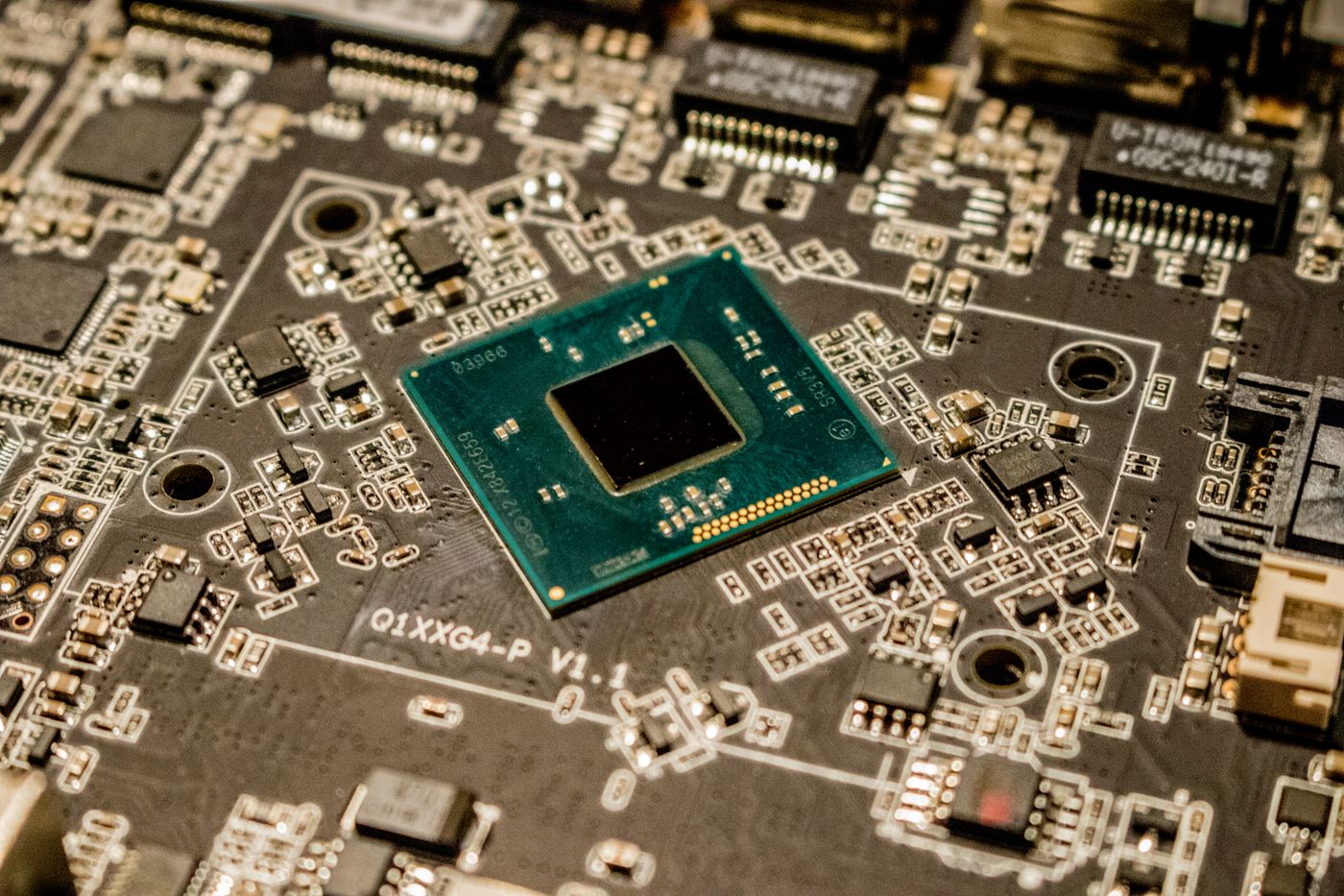
PCB design within the complete product.
SIDE connects circuit development and PCB layout with the software, enclosure, and operating requirements of your product. We support new board designs and help investigate problems in existing electronics.
Our approach begins with the intended function, available design information, and the constraints that matter to your application. Those requirements guide component choices, board architecture, and the integration plan.
From schematic to board layout
We develop schematics and translate connectivity into component placement and routing. Board outline, mounting points, connectors, and enclosure interfaces are considered alongside the electrical design.
Design & Layout
- Circuit architecture and schematic development
- Component selection and PCB placement
- Routing and board interface definition
- Mechanical outline and enclosure coordination
Build & Evaluation
- Assembly and test-access considerations
- Prototype board bring-up
- Hardware and firmware integration
- Troubleshooting and design revisions
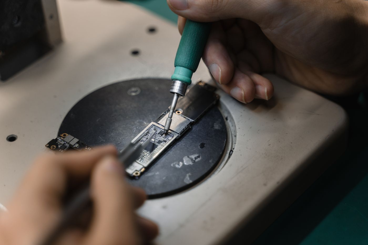
Design with the prototype in mind.
Placement and routing choices affect assembly, inspection, and access for measurement. We consider these needs during development so the prototype can help answer the right engineering questions.
Power, signal paths, component spacing, and thermal constraints are reviewed in the context of the agreed application.
A practical development sequence
- Define the board requirements. Clarify function, interfaces, dimensions, and evaluation goals.
- Develop the design. Coordinate circuitry, board layout, and mechanical fit.
- Integrate and evaluate. Bring up the prototype, investigate issues, and refine the design.
Bring us your next design challenge.
To start a conversation, share your current design stage and the issue you want to solve. Existing schematics, layout files, enclosure drawings, photos, and test observations help us understand the work.